
/h100-pci-e-3qtr-right-reverse_820x8202022102717053720240104142817.jpg)
Advantech
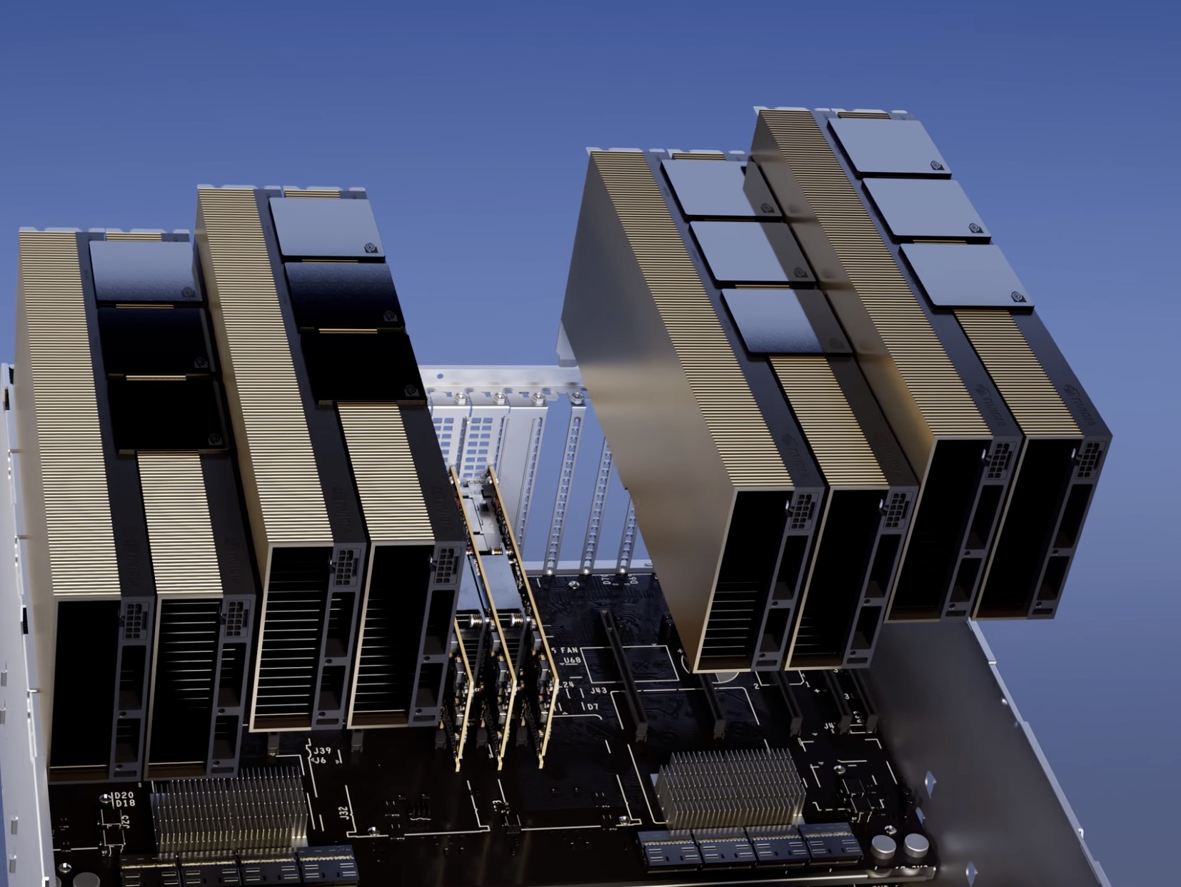
Web Rather at a total capacity of 188GB of memory theyre getting effectively 94GB per card NVIDIA hasnt gone into detail on this design quirk in our pre-briefing ahead of todays keynote. An Order-of-Magnitude Leap for Accelerated Computing Tap into exceptional performance scalability and security for every workload with the NVIDIA H100 Tensor Core GPU. Web The NVIDIA H100 NVL supports double precision FP64 single- precision FP32 half precision FP16 8-bit floating point FP8 and integer INT8 compute tasks The NVIDIA H100 NVL card is a dual. Web What we do know is that the H100 NVL will come with 94GB per GPU and 188GB HBM3 total We assume the missing 2GB per GPU is either for ECC or somehow related to yields. Web The new H100 NVL with 94GB of memory with Transformer Engine acceleration delivers up to 12x faster inference performance at GPT-3 compared to the prior generation A100..
An Order-of-Magnitude Leap for Accelerated Computing Tap into exceptional performance scalability and security for every workload with the NVIDIA H100 Tensor Core GPU. Web All told NVIDIA is touting the H100 NVL as offering 12x the GPT3-175B inference throughput as a last-generation HGX A100 8 H100 NVLs vs. Web NVIDIA NVLink is a high-speed point-to-point P2P peer transfer connection Where one GPU can transfer data to and receive data from one other GPU The NVIDIA H100 NVL card supports. Web Data SheetNVIDIA H100 Tensor Core GPU Datasheet This datasheet details the performance and product specifications of the NVIDIA H100 Tensor Core GPU. Web NVIDIA NVLink is a high-speed point-to-point P2P peer transfer connection Where one GPU can transfer data to and receive data from one other GPU The NVIDIA H100 card supports NVLink..
The Nvidia Hopper H100 GPU is implemented using the TSMC 4N process with 80 billion transistors It consists of up to 144 streaming multiprocessors. An Order-of-Magnitude Leap for Accelerated Computing Tap into unprecedented performance scalability and security for every workload with the NVIDIA H100 Tensor Core GPU. WebpageWhite PaperNVIDIA H100 Tensor Core GPU Architecture Overview WebpageData SheetNVIDIA H100 Tensor Core GPU Datasheet. The NVIDIA H100 GPU with a PCIe Gen 5 board form-factor includes the following units 7 or 8 GPCs 57 TPCs 2 SMsTPC 114 SMs per GPU 128 FP32 CUDA CoresSM 14592 FP32. Nvidia Reveals Hopper H100 GPU With 80 Billion Transistors Built on a custom TSMC 4N process..
The NVIDIA H100 NVL supports double precision FP64 single- precision FP32 half precision FP16 8-bit floating point FP8 and integer INT8 compute tasks The NVIDIA H100 NVL card is a dual. An Order-of-Magnitude Leap for Accelerated Computing. NVIDIA NVLink is a high-speed point-to-point P2P peer transfer connection Where one GPU can transfer data to and receive data from one other GPU The NVIDIA H100 card supports NVLink. The H100 NVL is an interesting variant on NVIDIAs H100 PCIe card that in a sign of the times and NVIDIAs extensive success in the AI field is aimed at a singular market. Data SheetNVIDIA H100 Tensor Core GPU Datasheet This datasheet details the performance and product specifications of the NVIDIA H100 Tensor Core GPU..
Servethehome


Comments